
Resonac (formerly Showa Denko) has successfully fabricated a 300mm (12‑inch) silicon carbide single crystal and completed substrate processing, the company announced in Japan. This represents the largest commercially viable single‑crystal diameter in the SiC semiconductor field today.
Resonac currently supplies 150mm (6‑inch) SiC epitaxial wafers as its main product, with 200mm (8‑inch) SiC epi wafers already shipping. SiC offers superior power conversion, thermal conductivity, and optical refraction properties, targeting applications in EVs, renewable energy, data center power, high‑heat‑density chips, and XR devices.
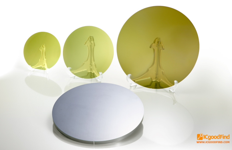
Larger SiC substrates enable more chips per wafer, effectively reducing per‑device manufacturing costs – a key direction for the power semiconductor industry.
ICgoodFind Takeaway:
Resonac's 12‑inch SiC breakthrough accelerates the industry's large‑format transition. For automotive and data center power devices, this could improve long‑term supply – buyers should track substrate and epi wafer volume ramp progress.
